Tuesday, March 22, 2011

Xilinx : Zynq-7000 Extensible Processing Platform

Is this the new trend for 2011 - FPGA and Micro Processor going hand in hand?
This time its ARM and Xilinx.


The Zynq™-7000 family is Xilinx's first Extensible Processing Platform (EPP). This new class of product combines an industry-standard ARM® dual-core Cortex™-A9 MPCore™ processing system with Xilinx unified 28nm architecture. This processor-centric architecture offers the flexibility and scalability of an FPGA combined with ASIC-like performance and power and the ease of use of an ASSP.

The four devices of the Zynq-7000 EPP family allow designers to target cost sensitive as well as high-performance applications from a single platform using industry-standard tools. The tight integration of the processing system with programmable logic allows designers to build accelerators and peripherals to speed key functions by up to 10x. ARM architecture and ecosystem maximizes productivity and eases development for software and hardware developers.


http://www.xilinx.com/technology/roadmap/zynq7000/features.htm

SOURCE - Xilinx : Zynq-7000 Extensible Processing Platform

Friday, March 18, 2011

A Match Made in Silicon Heaven?

A configurable Intel Atom processor with an on-package Altera FPGA

I stumbled across this article the other day and it got me thinking about what a big partnership this is and what impact it will have on the embedded world.

E600 brings everything onboard for the platform, including PCI-E for using the E600 in a multitude of different capacities. Either bring your own PCH or build one yourself - Intel already showed examples of Realtek, OKI, and ST Microelectronics on stage. If you're just building a desktop, Intel has a fairly standard platform controller hub called the EG20T for control like ethernet, SATA and USB. Intel really hopes that their embedded Atom platform will bring cost of system integration way down.

Ok So its a new ATOM CPU so what?

When designing a microprocessor you have two options. For very complex designs you have a bunch of engineers come up with an architecture. They then spend countless hours, days, months, eons designing it, and doing layout and performance optimization. Photolithographic masks are made and handed off to a fab that produces the silicon on wafers. This is a great approach for microprocessors that have high complexity, performance and volume demands. If you have a simpler design and want to get it to market cheaper, there's another option: a FPGA.

A field programmable gate array is exactly what it sounds like, a whole bunch of gates on a die that can be programmed in the field. An FPGA can be made to function like pretty much whatever microprocessor design you program it to be. You shave off the initial manufacturing costs as you don't need to make expensive masks. FPGAs are often used in emulating larger microprocessor designs.


As Intel tries to take the Atom into the embedded space it may run into some customers that want to pair Atom with custom hardware. Intel could simply make a version of Atom for every single market vertical, however that would incur a significant cost overhead. 

Instead, in the first half of 2011 Intel will introduce the Stellarton processor. It's a configurable Intel Atom processor with an on-package Altera FPGA.

The theory sounds great but in practice this could be tricky device to integrate - don't you think?

SOURCE - AnandTech , SLASHGEAR, Intel

Friday, March 11, 2011

ZX81: Small black box of computing desire

ZX81

The Sinclair ZX81 was small, black with only 1K of memory, but 30 years ago it helped to spark a generation of programming wizards.

Packing a heady 1KB of RAM, you would have needed more than 50,000 of them to run Word or iTunes, but the ZX81 changed everything.

It didn't do colour, it didn't do sound, it didn't sync with your trendy Swap Shop style telephone, it didn't even have an off switch. But it brought computers into the home, over a million of them, and created a generation of software developers.

Before, computers had been giant expensive machines used by corporations and scientists - today, they are tiny machines made by giant corporations, with the power to make the miraculous routine. But in the gap between the two stood the ZX81.


SOURCE - BBC News - ZX81: Small black box of computing desire

Tuesday, March 1, 2011

Embedded World - 2011


The embedded world Exhibition&Conference is the world´s biggest exhibition of its kind and the meeting-place of the international embedded community. Embedded technologies are in action everywhere -whether in the car, data and telecommunication systems, industrial and consumer electronics, military systems or aerospace.


The embedded world Exhibition&Conference is the top get-together for the international embedded community. The exhibition set another record in 2010 with 730 exhibiting companies, and more than 18,000 trade visitors used the opportunity to obtain a comprehensive picture of the latest embedded technology trends.

Will you be going?
Are you already there?
What are you looking for at EW2011?

Visit the Exhibition Website - Embedded World

Monday, February 14, 2011

Freescale QorIQ P4080 / XPedite 5470

QoriQ P4080 (P4 Series)

The QorIQ P4080 processor, the first product offered in the QorIQ P4 platform series, delivers industry leading performance in the under 30-watt power category. It combines eight Power Architecture™ e500mc cores – operating at frequencies up to 1.5 GHz – with high-performance datapath acceleration logic, and network and peripheral bus interfaces. All this designed for 45nm technology to deliver high-performance, next-generation networking services in a very low power envelope.

The QorIQ P4080 processor can be used for combined control, datapath, and application layer processing. Its high level of integration offers significant performance benefits compared to multiple discrete devices, while also greatly simplifying board design. The processor is well-suited for applications that are highly compute-intensive, I/O intensive, or both, making it ideal for applications such as enterprise and service provider routers, switches, base-station controllers radio network controllers (RNCs), longterm evolution (LTE) and general-purpose embedded computing systems in the networking, telecom/datacom, wireless infrastructure, military and aerospace markets.

Source - http://www.freescale.com/webapp/sps/site/prod_summary.jsp?code=P4080

Extreme Engineering Solution XPedite 5470

The XPedite5470 is a high-performance 3U VPX-REDI single-board computer based on the Freescale P4080 processor. With eight PowerPC e500 cores running at up to 1.5 GHz, the P4080 delivers enhanced performance and efficiency for today's embedded computing applications.

The XPedite5470 supports two separate channels of up to 4 GB each of up to DDR3-1333 ECC SDRAM, as well as up to 16 GB of NAND flash and up to 256 MB of NOR flash (with redundancy). The XPedite5470 provides the option of utilizing a PCI Express or Serial RapidIO Fat Pipe P1 interconnect, as well as two SerDes Gigabit Ethernet Thin Pipe P1 fabric interconnects. The XPedite5470 also supports dual Gigabit Ethernet, GPIO, I²C, PMC I/O, XMC I/O, and up to two RS-232/RS-422/RS-485 serial ports through the P2 connector.

The XPedite5470 provides a ruggedized, high-performance, feature-rich solution to support the next generation of rugged embedded applications. Wind River VxWorks, QNX Neutrino, Linux, and Green Hills INTEGRITY Board Support Packages (BSPs) are available.

Source - http://www.xes-inc.com/Products/XPedite5470/XPedite5470.html

Monday, February 7, 2011

Altera Wants You...


Altera Corp want your opinions and input. Set up in 2010 the Altera Wiki was founded to provide a website for Altera users to contribute technical how-to articles and share their projects and IP with the community for all Altera related topics. The Altera Wiki complements the Altera Forum site. The Altera Forum is still the site to use for Question and Answer community help using thread discussions.


The Altera Wiki is a dynamic library of public articles that any and all can update and contribute. They have integrated the Nios Wiki into the Altera Wiki, including all pages and usernames. If you have any trouble accessing your account, please contact the Admin (wikiadmin 'at' alterawiki 'dot' com). To be a contributor to existing or create new article or project share, just register for a free account and sign in.


What is a WIKI?

A wiki is a collaborative Web site oriented to providing knowledge in a particular domain. Anyone can enter information, or change or comment on anyone else's contributions. A wiki website allows communities to easily create and edit web pages via a web browser using a WYSIWYG text editor or simplified language called wikitext.

Wikipedia definition: A wiki is a website that allows the easy creation and editing of any number of interlinked web pages via a web browser using a simplified markup language or a WYSIWYG text editor.Wikis are typically powered by wiki software and are often used to create collaborative wiki websites, to power community websites, for personal note taking, in corporate intranets, and in knowledge management systems.


SOURCE : Altera Wiki , See also - http://www.alteraforum.com/

Friday, February 4, 2011

MIL-STD-1553 Interfaces for Data Acquisition

MIL-STD-1553

Originally published by the U.S. Department of Defense (DOD) in 1973, MIL-STD-1553 is a military standard defining the mechanical, electrical, and functional characteristics of a serial data bus. Originally defined for military avionics, MIL-STD-1553 has become common in both military and civil spacecraft data handling subsystems.

DNx-553-1553: MIL-STD-1553 Interfaces The
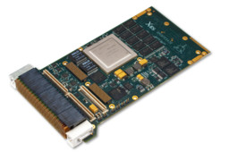
 DNA-1553-553 and DNR-1553-553 are high-performance, two-channel MIL-STD-1553 interfaces for UEI’s popular “Cubes” and RACKtangle I/O chassis respectively. Each port operates fully independently and provides a complete dual, redundant 1553 interface and may be set as 1553a or 1553b. The “b” interface fully implements specification notices 1 and 2. Each port is transformer coupled, though direct coupling is available as an option.

Many 1553 functions are implemented in an on-board FPGA. This greatly reduces the burden placed on the chassis CPU and ensures the DNx-1553-553 does not interfere with the functionality of other I/O boards installed.

Each port may be independently configured as Bus Controller (BC), Remote Terminal (RT) or Bus Monitor (BM). As Bus Controller, the board supports all standard BC-RT, RT-BC and RT-RT transfers. The Remote Terminal support allows the board to emulate up to 31 different RTs on the bus. Bus Monitoring (BM) mode provides the ability to monitor all activity, or selective activity based upon RT address. In addition to monitoring data, BM monitors time tags, error status and RT response time. Finally, each DNA-1553-553 channel may be set to simultaneously act as an RT and BM or BC and BM.

MIL-STD-1553


MIL-STD-1553

When installed in the Cube, the DNA-1553-553 is well suited for the harsh environments sometimes encountered in flight testing applications. The board is specified for operation from -40° to +85° C, from 0 to 70,000 feet. The system is also fully tested for operation at 5g vibration and up to 50 g shock.
The DNx-1553-553 includes a standard MIL-1553 cable interface. Also included is a helpful, self-test loop-back adaptor.

The DNA/DNR-1553-553 includes our 1553 API, designed to offer simple, easy-to-use controls and yet maintain the ability to access all 1553 functionality. The software driver is compatible with all popular operating systems including Windows Vista and XP and Linux as well as most real-time OS’s such as RTX, QNX, RT Linux and more. Software support is also included for all popular programming languages and data acquisition (DAQ) application packages including LabVIEW and MATLAB.

SOURCE - http://www.ueidaq.com/mil-std-1553


UEI is a leader in the PC/Ethernet data acquisition and control, Data Logger/Recorder and Programmable Automation Controller (PAC) and Modbus TCP markets. Our revolutionary “Cube” form factor provides a compact, rugged platform, ideal for applications in the automotive, aerospace, petroleum/refining, simulation, semiconductor manufacturing, medical, HVAC, power generation and more.

The “Cube” is uniquely flexible, capable of being deployed as an Ethernet I/O slave, a standalone data logger, a standalone Linux-based PAC or a Modbus Slave. The “Cube” also offers incredible I/O flexibility, accommodating up to 6 I/O boards from a selection of over 25. This allows you to precisely match the I/O configuration to your application. With I/O interfaces for analog I/O, digital I/O, counter/timer, ARINC-429, quadrature encoder, CAN-bus, serial I/O and more, we are sure to have the interface you need.

Thursday, February 3, 2011

Altera's 28-nm Variable-Precision DSP Block Architecture Wins the 2011 DesignVision Award


Altera Corporation (NASDAQ: ALTR) has announced that its variable-precision digital signal processing (DSP) block architecture won the DesignCon 2011 DesignVision Award in the Semiconductor and IC category. Altera's variable-precision DSP block architecture was recognized by DesignVision Award judges for its ability to enable high-precision, high-performance digital signal processing in FPGAs that efficiently supports many different precision levels. This unique architecture is implemented within Altera's portfolio of 28-nm FPGAs to increase system performance, reduce power consumption and reduce architecture constraints for DSP algorithm designers. Altera was presented with the 2011 DesignVision Award at a ceremony held at the Santa Clara Convention Center during DesignCon 2011.


Altera developed the industry's first variable-precision DSP block architecture to meet the industry's demands for higher precision signal processing. This innovative architecture allows each DSP block in the FPGA to be configured at compile time to three 9x9, two 18x18 or a single 27x27 or 18x36 multiplier mode. Additional higher precision modes are available using multiple DSP blocks. This architecture supports, on a block-by-block basis, various precisions per block, ranging from low resolution fixed point video up to single-precision floating point within a single DSP block, and even double-precision floating point with minimal external logic. To learn more about Altera's variable-precision DSP block architecture, or to view a white paper or webcast on the architecture, visit www.altera.com/dsp-variable-precision.

SOURCE - Altera's 28-nm Variable-Precision DSP Block Architecture Wins the 2011 DesignVision Award

Has VME Learned From xTCA?

Altera Stratix® IV GX AdvancedMC from BittWare

Late in 2002, PICMG released the first version of the Advanced TeleCommunications Architecture (ATCA) standard. This defined the first true blade-based architecture, wherein all communication across the backplane was via a high-speed serial switch fabric, rather than over a shared, parallel, multidrop bus. This was followed by the Advanced Mezzanine Card (AMC) standard in 2005.

It didn’t take folks that long to realize that AMC cards could also be used as blades in smaller footprint systems. PICMG released the first version of the resultant MicroTCA standard in 2006. The advent of MicroTCA was seen as a positive development for the market, not only because of its technical capability and reduced footprint (vs. ATCA), but because it also expanded the potential market for AMC cards. These could be used either as mezzanine cards or as MicroTCA blades, yielding higher potential volumes and thus greater economies of manufacturing scale.

The VME industry was slower to adopt blade-based systems architectures, largely because military and aerospace defines the primary market for VME systems, and the military tends to take a more cautious approach to innovation than do civilian markets. In the latter, time-to-market is of overarching concern, whereas in military and aerospace, where mission criticality is the primary concern, far more emphasis is placed on reliability and ruggedness.

However, the evolution of VME through VME2eSST and VXS to VPX and OpenVPX has brought blade architectures, similar to ATCA, to the forefront of VME-based technology. It now appears that parallels to AMC and MicroTCA are also in the works.


Two new small form factor systems architectures are currently being investigated by VITA, with the objective of producing standards. These are “micro.VPX”and “NanoATR.” The former is the brainchild of PCI-Systems, Inc., and is the subject of working group VITA 73; it utilizes a small form factor VPX card. The latter, NanoATR, was developed by Themis Computer, targeted at ATR systems for aircraft, and utilizes an even smaller card. NanoATR is the subject of working group VITA 74. Both versions of the cards are being evaluated by the VITA 71 working group, which is developing a standard for a new rugged VME mezzanine architecture.

Source - VDC Research: Embedded Microprocessor, Board & Systems Market Blog

Wednesday, February 2, 2011

VPX & OpenVPX Technology from Extreme Engineering Solutions

VPX Rugged Boards from X-ES

X-ES is an industry and technology leader with regard to VPX and OpenVPX™. X-ES was actively involved in the development of the VPX and OpenVPX standardization efforts. X-ES was one of the first companies to develop VPX products and has been shipping VPX products since 2006.

VPX Specification

VPX (VITA 46), a module standard, was developed in support of ruggedized, deployed applications and is the technology of choice for ruggedized military applications where Size, Weight, and Power (SWaP) are an issue. VPX supports both 3U and 6U form factors, provides a large amount of high-speed I/O to the backplane, and enables the use of modules that require up to 200 watts of power.

VPX-REDI Specification

The Ruggedized Enhanced Design Implementation (REDI) laid out in VITA 48 defines how to implement cooling methodologies on specific board form factors. It supports enhanced forced-air cooling (using baffles and plenums), advanced conduction cooling (using larger and more efficient thermal interfaces), and liquid cooling. It also addresses the use of ESD covers on both sides of the board, a necessary feature for military two-level maintenance strategies.

OpenVPX™ Specification

OpenVPX™ (VITA 65) builds on the module-centric VPX specifications by providing a nomenclature of planes and profiles to enable system integrators, module designers, and backplane providers to effectively describe and define aspects and characteristics of a system. OpenVPX addresses major system interoperability issues while allowing for flexibility within the system, as enabled by its planes and flexible module profiles featuring user-defined I/O. By following a system-centric approach and defining a number of standard system topologies, OpenVPX enables interoperable off-the-shelf modules and development platforms within the VPX marketplace.

OpenVPX profiles make is easy to build development systems with compatible components. Deployable systems will always have system issues that need to be addressed, such as I/O, custom backplanes, power, and cooling. X-ES not only understands these issues, but has solved integration and system-level problems and delivered integrated VPX system solutions to customers.


X-ES provides a comprehensive line of 3U and 6U VPX products, including Intel®-based and PowerPC-based Single Board Computers (SBCs), carriers, switches, and I/O cards for embedded computing applications.

Because the environmental and SWaP constraints associated with rugged, deployed solutions complicate the design and integration of these systems, X-ES provides additional system-level components such as backplanes, power modules, development platforms, and deployable systems.

For more details and to view the range of VPX and OpenVPX products visit -
VPX and OpenVPX™ Technology - Extreme Engineering Solutions, Inc

Tuesday, February 1, 2011

Intel Sandy Bridge Processors & Embedded Computers

Intel Sandy Bridge

There has been a lot of talk regarding the "2nd generation Intel® Core™ processor family," previously known as Sandy Bridge. Some of the talk out there contains a bit of hype, but the reality is there are some major design changes to the processor in the Sandy Bridge architecture that will vastly improve single board computer, embedded motherboard and industrial computer system performance, power efficiencies and platform security.
Industrial computing solutions deployed in Mil-COTS defense applications, medical imaging and industrial automation systems are well suited to take full advantage of Sandy Bridge micro-architecture features. Trenton is hard at work developing a single processor system host board based on Sandy Bridge technology and expects to have evaluation units available by the end of Q1!

The way the processor sections on the Sandy Bridge CPU die have been re-ordered in this new architecture provides a tighter integration between the memory interface, processing cores and the traditional Northbridge functions. This is being argued as the first major, ground up x86 processor design since the Intel® Pentium® Pro was introduced back in the early '90s. That is the not Intel® hype per se, but in going though the re-ordering and re-structuring of the CPU die in Sandy Bridge, we can see validity of the claim that Sandy Bridge processors should provide a significant performance boost compared to the previous generation Westmere class of CPUs at a sharply reduced power consumption.

The Sandy Bridge architecture provides multiple processing cores with up to eight cores in the processor versions scheduled for release later this year and into the early part of next year. In addition to the processor cores, there is a separate graphics core and a new processor feature called Intel® AVX. AVX stands for Advanced Vector Extensions and it improves floating point computational speeds. A doubling of the vector widths to 256 bits and the ability to process partial width load and store operations also helps this AVX capability to boost performance.

Semiconductor Die Image

All of this gets combined with a new capability of applying Intel® Turbo Boost Technology across all cores; including the graphics core, to dynamically boost selected core processing frequencies based on the demands of the system at any given time. This should boost high-def video and 3-D graphics performance in video processing applications. One of the other improvements in Sandy Bridge is the ability to use these new processor architecture features to support multiple video and 3D graphic interfaces directly out of the processor.

Benchmark testing for our future board and system designs will confirm and quantify just how much of a performance boost to expect in your industrial computer applications using Sandy Bridge technology. Trenton's first Sandy Bridge-based SBC will be introduced next month and supports some interesting features such as dual video interfaces and a mini-PCI Express connector to support industry standard mini-PCIe cards. Stay tuned for future Trenton developments or give your Trenton account manager a call at 770.287.3100 or 800.875.6031 for additional information.

This submission is by Jim Renehan, Director of Marketing at Trenton Technology


SOURCE - Are Sandy Bridge Processors & Embedded Computers a Good Fit?

Monday, January 31, 2011

What have SONY put into their new handheld?

ARM Cortex 9
For the next generation PSP - PSP2 or NGP - Sony has abandoned the internally developed MIPS architecture that powered the PSP, and has opted for an ARM processor, with a PowerVR graphics processing unit. This puts the machine inline with massive majority of high-end smartphones: ARM reckons 95% of all current mobile handsets have application processors based on its IP, while Imagination Technologies, the developer of the PowerVR graphics chipset, claims 200 current models feature its technology. ARM and PowerVR chips are in the Apple iPad as well as high profile Google handsets such as the Galaxy S.

Cortex-A9 Processor

The ARM Cortex™-A9 processor provides unprecedented levels of performance and power efficiency making it an ideal solution for designs requiring high performance in low power or thermally constrained cost-sensitive devices.

Available as either a single core or configurable multicore processor, with both synthesizable or hard-macro implementations available. This processor can scale across a wide variety of applications while enabling a consistent software investment across multiple markets.

The Cortex-A9 processors are the highest performance ARM processors implementing the full richness of the widely supported ARMv7 architecture. Designed around the most advanced, high efficiency, dynamic length, multi-issue superscalar, out-of-order, speculating 8-stage pipeline, the Cortex-A9 processors deliver unprecedented levels of performance and power efficiency with the functionality required for leading edge products across the broad range of consumer, networking, enterprise and mobile applications.

The Cortex-A9 microarchitecture is delivered within either a scalable multicore processor, the Cortex-A9 MPCore™ multicore processor, or as a more traditional processor, the Cortex-A9 single core processor. Supporting the configuration of 16, 32 or 64KB four way associative L1 caches, with up to 8MB of L2 cache through the optional L2 cache controller, the scalable multicore processor and the single processor provide the broadest flexibility and are each suited to specific applications and markets.